Search
Close this search box.

Follow us!

Electronics

Lasery do produkcji układów elektronicznych
Laser technology is one of the primary manufacturing methods accompanying the production of electronic circuits. It is thanks to it that it is possible to weld, cut, drill and mark individual components and final products with high quality and high processing efficiency.
The electronics industry is not only copper or iron alloys, but also composites and plastics. High-volume production means that high reliability and high process speed are required, which fits perfectly with the characteristics of laser processing. It is features such as non-contact operation, precision and repeatability that make the laser is the ideal tool for this type of process, definitely distinguishing itself from conventional manufacturing methods.

Ablation

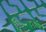
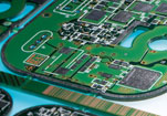
The use of laser micromachining, particularly the ablation technique, allows precise, controlled removal of successive layers of material. The laser beam, controlled by a scanning head, travels along the surface of the part, vaporizing the plastic that shields and insulates the electrical paths. By properly controlling the power and operating speed, the face of the conductor remains intact, and the repeatability and speed of the focus positioning makes it possible to process multiple components at once.

Cutting

Laser beam cutting brings a lot of advantages to the electronics industry, since it’s what makes it possible to process almost any material without worrying about tool wear. Great freedom in the design of even complex shapes is not an obstacle for the laser due to the considerable freedom of beam guidance and the high speed of shape cutting. In addition, the use of scanning heads allows for shorter focus positioning times, enabling processing of components on the production line.

Welding

Laser welding, in the case of the electronics industry, involves making spot or line welds. The precision and repeatability of the process make it possible to permanently join even the smallest components with the help of this technique – whether they are housing fragments or battery cells. The speed at which the welds are made means that the amount of heat supplied to the material is minimal, which is important for sensitive electronics. In addition, the use of the laser increases production flexibility, as the system can easily be reprogrammed as needed, and the use of scanning heads ensures that multiple parts can be joined at once. The option of joining plastics that are transparent to the laser creates the possibility of creating welds at the interface between two materials when one component is on top of another. The minimal heating of the component, the intact surface of the material and the high strength of the joint make laser technology far superior in this regard to classic techniques such as welding.

Drilling

A PCB is a composite consisting of both an electrical conductor and a dielectric layer, as well as a core that gives rigidity to the laminate. The diversity of materials used means that conventional manufacturing methods could cause damage to the board during processing, such as crushing or cracking. Thanks to the non-contact nature of laser technology, the high precision of the process and the minimal mechanical stress on the workpiece, drilling holes in electronic circuits does not cause damage or defects. With laser drilling, it is possible to obtain holes for integrating the board into the housing, as well as channels that provide an electrical connection between successive conductive layers.

Marking

Marking electronic circuit boards, silicon wafers and numeric keyboards or making markings on enclosures are just some examples of laser applications for marking components in the electronics industry. Compared to conventional methods, laser technology is characterized by the ability to apply codes and symbols on very small surfaces – even as small as 1 mm x 1 mm – while maintaining high quality and accuracy throughout the process. Moreover, there is no mechanical or thermal stress, which is important from the point of view of electronic components. Moreover, thanks to the high speed of the process, it is possible to mark many components at once.
Among laser marking techniques, there are two basic methods:
  • annealing used in marking processes for parts made of metal, decolorization or
  • foaming in the case of parts made of plastic.
Scroll to Top